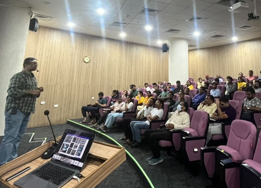
Dr Naresh Emani’s research revolves around semiconductors that are building blocks of tiny chips that drive our electronic devices. His recent OpenLab talk offered a ringside view of the field, from the miniscule scale of these chips and the futuristic technologies enabling their precise fabrication to the ebbs and flows of the semiconductor industry that spills over to global geopolitics. Here are some snapshots.
Transistors are getting smaller
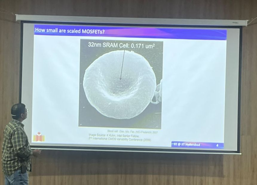
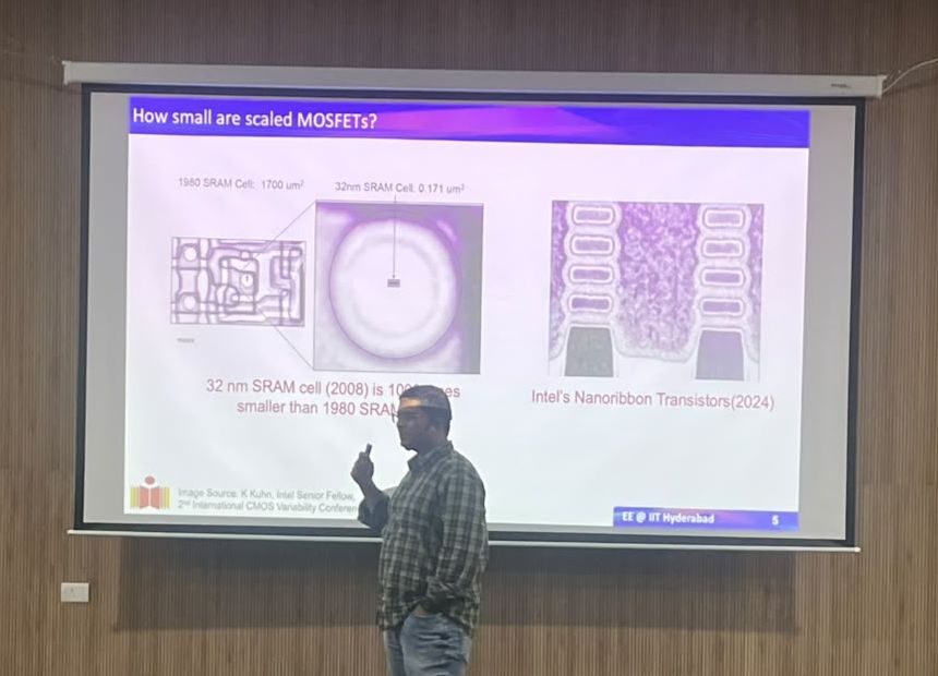
Transistors are semiconductor devices that form the building blocks of processors powering our electronic devices. Before the transistors were invented in the 1940s, less than a centimeter in size, computers used bulky vacuum tubes that spanned entire rooms. Since then, transistors have continued to shrink over the decades, where today, a processor about 1.5 x 1.5 cm in size may be packed with over 60 billion tiny transistors, speeding up computation. For a sense of scale, the MOSFET switch (marked by an arrow in the image) is a small fraction of the size of a red blood cell (large white concave disc).
The cleanest room you can imagine
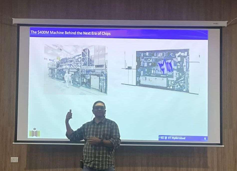
Making nanoscale semiconductor devices that we cannot even see using the naked eye needs an ultra-clean environment and tools of extraordinary precision. Their fabrication is so sensitive that winds carrying dust particles, or the rumble of a train hundreds of meters away can lead to defects. With chips getting smaller, extremely powerful machines are needed to fabricate them. The Dutch company ASML makes lithography machines (seen in the image) that use extreme ultraviolet light to make nanoscale patterns on silicon wafers. The light is generated using plasma heated to temperatures several times hotter than the surface of the Sun.
Keeping up with Moore’s law
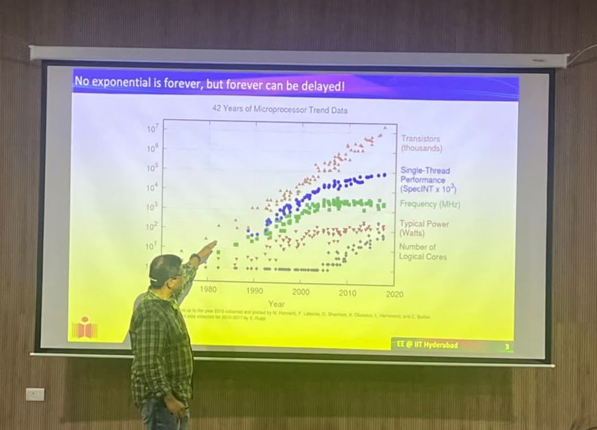
Since the 1970s, advances in fabrication technology have enabled the number of transistors on a microchip to roughly double every two years, an observation known as Moore's law. During this rapid evolution, the path has not always been clear. Scientists test different ideas up their sleeve, but it is hard to predict which of these would prove successful. While the number of transistors on a microchip has continued to rise, processor performance (blue dots in the image) has plateaued since the 2000s, which continues to be a challenge. Various aspects of this are being addressed by researchers around the world, including at IIT Hyderabad.
A high-stakes race
Researchers are now developing three-dimensional transistors by stacking nanoscale ribbons (image on right) while also exploring approaches such as spintronics, magnetic memory, photonics and quantum computing. These ideas have immense commercial value and are closely guarded by companies. Strategic decisions made in this field have far-reaching consequences for national economies as revenue from semiconductors can fuel more research and innovation. While India has contributed significantly to semiconductor design in the past, the India Semiconductor Mission is investing heavily in domestic manufacturing, which has the potential to transform the economy.
A clean room of one’s own
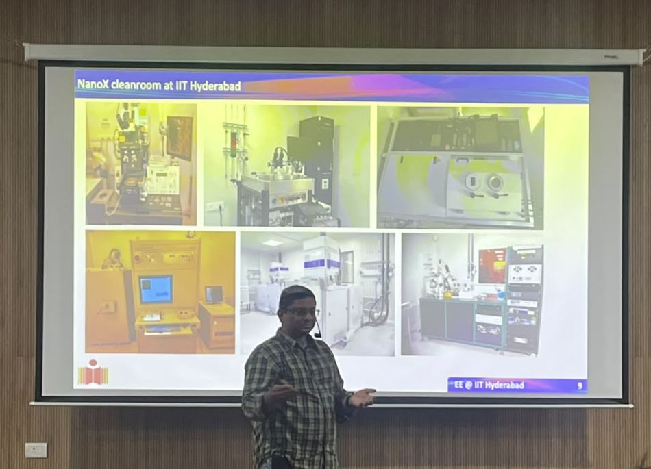
The NanoX facility at IIT Hyderabad spans 2000 sq ft, with two clean rooms housing cutting-edge equipment used in semiconductor research and fabrication. It has machines for lithography to transfer nanoscale patterns on substrates, evaporation and sputtering to deposit extremely thin metal layers, etching to engrave structures into substrates and wet processing. The facility also supports integrating and packaging different components into chips and characterisation to evaluate device performance.
Investing in the workforce of tomorrow
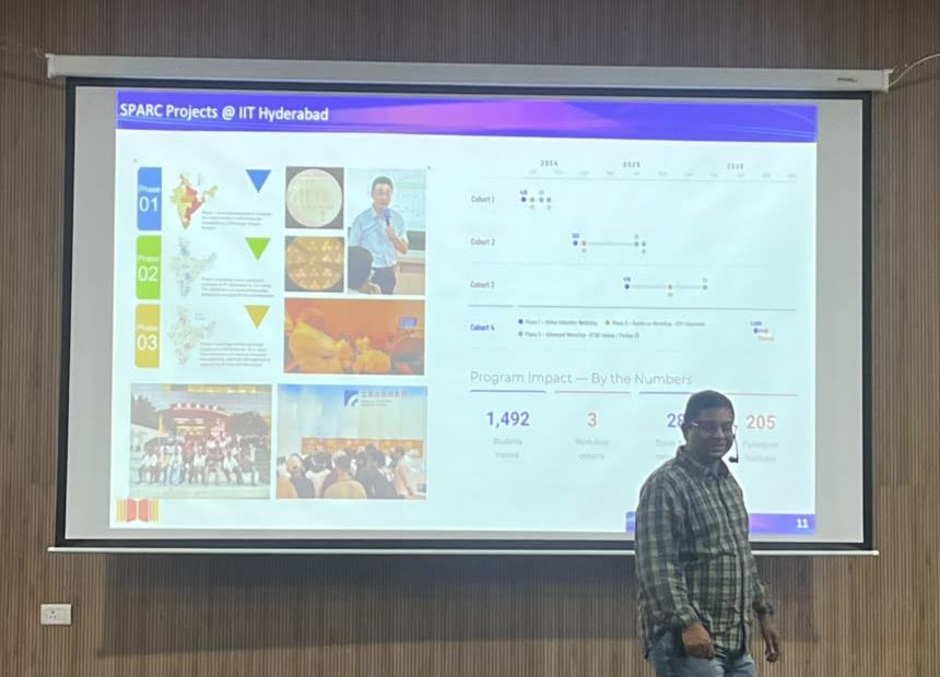
The SPARC-NanoX project at IIT Hyderabad trains students in semiconductor fabrication to create a skilled workforce for the emerging industry. Supported by the Ministry of Education, the program has introduced over 1400 students to semiconductor manufacturing through lectures from experts from India and abroad. Of these, around 175 students have spent two weeks on hands-on training in semiconductor fabrication in the NanoX facility on campus. Around 114 of these students visited fabrication facilities in the US or Taiwan for an immersive experience on the fab floor. Currently, a cohort of 38 students from across India are undergoing hands-on training at IITH.